- 4E, No.3 Shenfeng Road, Liuyao Community, Henggang Street, Longgang District, Shenzhen,China
- cc.shen@xypltd.com
- Call: +86 15112667855
Integrated Circuits (ICs)
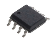
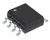
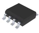
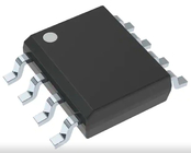
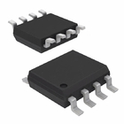
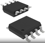
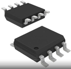
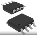
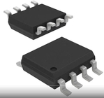
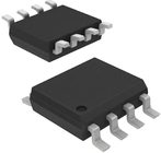
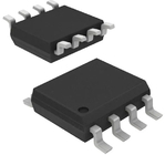
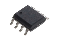
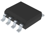
ICL7660AIBAZA-T Charge Pump Switching Regulator IC Positive Or Negative Fixed -Vin 2Vin 1 Output 45mA 8-SOIC
The ICL7660S and ICL7660A Super Voltage Converters are monolithic CMOS voltage conversion ICs that ensure significant performance advantages over other similar devices. They are direct replacements for the industry standard ICL7660 offering an extended operating supply voltage range up to 12V, with lower supply current. A Frequency Boost pin has been incorporated to enable the user to achieve lower output impedance despite using smaller capacitors. All improvements are highlighted in the “Electrical Specifications” section on page 3. Critical parameters are ensured over the entire commercial and industrial temperature ranges. The ICL7660S and ICL7660A perform supply voltage conversions from positive to negative for an input range of 1.5V to 12V, resulting in complementary output voltages of -1.5V to -12V. Only two non-critical external capacitors are needed, for the charge pump and charge reservoir functions. The ICL7660S and ICL7660A can be connected to function as a voltage doubler and will generate up to 22.8V with a 12V input. They can also be used as a voltage multipliers or voltage dividers. Each chip contains a series DC power supply regulator, RC oscillator, voltage level translator, and four output power MOS switches. The oscillator, when unloaded, oscillates at a nominal frequency of 10kHz for an input supply voltage of 5.0V. This frequency can be lowered by the addition of an external capacitor to the “OSC” terminal, or the oscillator may be over-driven by an external clock. The “LV” terminal may be tied to GND to bypass the internal series regulator and improve low voltage (LV) operation. At medium to high voltages (3.5V to 12V), the LV pin is left floating to prevent device latchup. In some applications, an external Schottky diode from VOUT to CAP- is needed to ensure latchup free operation (see Do’s and Dont’s section on page 8).
Features
• Ensured Lower Max Supply Current for All Temperature Ranges
• Wide Operating Voltage Range: 1.5V to 12V
• 100% Tested at 3V
• Boost Pin (Pin 1) for Higher Switching Frequency
• Ensured Minimum Power Efficiency of 96%
• Improved Minimum Open Circuit Voltage Conversion Efficiency of 99%
• Improved SCR Latchup Protection
• Simple Conversion of +5V Logic Supply to ±5V Supplies
• Simple Voltage Multiplication VOUT = (-)nVIN
• Easy to Use; Requires Only Two External Non-Critical Passive Components
• Improved Direct Replacement for Industry Standard ICL7660 and Other Second Source Devices
• Pb-Free Available (RoHS Compliant)
Applications
• Simple Conversion of +5V to ±5V Supplies
• Voltage Multiplication VOUT = ±nVIN
• Negative Supplies for Data Acquisition Systems and Instrumentation
• RS232 Power Supplies
• Supply Splitter, VOUT = ±VS
Functional Block Diagram
specification of ICL7660AIBAZA-T
|
Category |
Integrated Circuits (ICs) |
|
Function |
Ratiometric |
|
Output Configuration |
Positive or Negative |
|
Topology |
Charge Pump |
|
Output Type |
Fixed |
|
Number of Outputs |
1 |
|
Voltage - Input (Min) |
1.5V |
|
Voltage - Input (Max) |
12V |
|
Voltage - Output (Min/Fixed) |
-Vin, 2Vin |
|
Current - Output |
45mA |
|
Frequency - Switching |
3kHz |
|
Synchronous Rectifier |
No |
|
Operating Temperature |
-40°C ~ 85°C (TA) |
|
Mounting Type |
Surface Mount |
|
Package / Case |
8-SOIC (0.154", 3.90mm Width) |
|
Supplier Device Package |
8-SOIC |

