
- 4E, No.3 Shenfeng Road, Liuyao Community, Henggang Street, Longgang District, Shenzhen,China
- cc.shen@xypltd.com
- Call: +86 15112667855
News
Once the circuit design and materials are complete, PCB clearance is all that's left for these external plugins!
- 2026-10-13
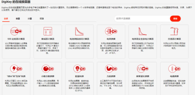
From product conception, theoretical and circuit design, component selection to physical production, every step is interrelated. It seems that the circuit diagram design is perfect and the material selection is determined, but in the end, there are many limitations and difficulties encountered in the production of printed circuit boards (PCBs). Which step went wrong? Should we reselect materials or redesign? In DigiKey's powerful tool library, as long as you make good use of some small tools, reduce errors and troubles, electronics and engineering become proficient. Next, we will introduce several design level tools that can help you easily create products.
Printed Circuit Board (PCB) Design
After the circuit simulation test of the solderless test board, the next step is the PCB circuit design. PCB is a sandwich board composed of insulation layer and conductive copper layer, which includes signal routing, power supply and grounding layers. The layout design of routing is as strict as the design of circuits, and the overall system needs to be considered. At the same time, it is necessary to understand the characteristics of the circuit in order to make corresponding circuit designs. Understanding the routing characteristics can assist engineers in quickly determining the PCB's circuit and layer requirements. Refer to the checklists for PCB design for the following two different systems.
The following is a sensing system using a 12-BIT microcontroller, which includes analog-to-digital (A/D) conversion, LCD display, and 5V external power supply in its circuit. Although the current carrying capacity is not high, the routing design of analog and digital circuits requires independent separation, and its checklist is used as a reference.
1. Check the position of the device and connector. Ensure that the high-speed device and digital device are close to the connector.
2. There must be at least one ground plane on the circuit board.
3. Make the power supply wiring wider than other wiring on the circuit board.
4. Check the current return path and look for possible noise on the grounding connection.
5. Properly bypass all devices. Place the capacitor as close as possible to the power pin of the device.
6. Keep all wiring as short as possible.
7. Track all high impedance traces and identify potential capacitive coupling issues between traces.
8. Ensure that the signals in the mixed signal circuit are filtered correctly.
(Source: Microchip)
And some basic rules for PCB circuit design to create a high current power controller using MOSFETs. Due to different current carrying requirements in different line areas, cost-effectiveness can also be considered in designing lines for different regions.
When designing power supply for slots, the parts should be placed together in a centralized manner.
Provide sufficient current to the load.
Noise resistance of load and detection circuits.
Consideration of current induction.
Consider heating up.
Consider the impedance of the wiring to reduce the derating impact on the high current track group.
(Source: Texas Instruments)
From the two completely different types of product designs mentioned above, it can be seen that there are certain requirements for the width of the wiring, including temperature changes, current carrying capacity, and impedance values. Next, we will introduce some small tools related to PCB design to assist you in quickly calculating the required wire width and wire impedance.