
- 4E, No.3 Shenfeng Road, Liuyao Community, Henggang Street, Longgang District, Shenzhen,China
- cc.shen@xypltd.com
- Call: +86 15112667855
News
Using MPS SiC diodes to minimize losses in high-frequency switch mode power supplies
- 2026-09-29
High frequency switch mode circuits, such as power factor correction (PFC) circuits using continuous conduction mode (CCM), require diodes with low switching losses. For traditional silicon (Si) diodes using CCM mode, these switching losses come from the reverse recovery current generated by the charge stored in the diode junction when the diode is turned off. To minimize these losses, a Si diode with a higher average forward current is usually required, but this leads to larger size and higher cost.
In CCM PFC circuits, silicon carbide (SiC) diodes are a better choice because their reverse recovery current is essentially only capacitive current. Reducing the injection of minority carriers in SiC devices means that the switching loss of SiC diodes is close to zero. In addition, merging PIN Schottky (MPS) SiC diodes can reduce the forward voltage drop of the device, similar to traditional SiC Schottky diodes. This will further minimize the conduction loss.
This article first briefly discusses the challenges faced by low loss switches in CCM PFC circuits. Then introduce an example of a MPS device from Vishay General Semiconductor - Dior Division and explain how to apply the device to minimize losses.
Low loss switch requirements
AC/DC switching power supplies with a rated power exceeding 300 W typically use PFC to meet international standards such as IEC61000-4-3, which specify reactive power and line harmonic levels. The diodes used in PFC power supplies, especially those used in high-frequency switching power supplies, must be able to withstand the rated power of the power supply and the losses related to circuit conduction and switching actions. Si devices exhibit significant reverse recovery losses. When switching from a conductive state to a non-conductive state, Si diodes will maintain a conductive state while the charged carriers are removed from the junction. This will cause a large amount of current to be generated during the reverse recovery time of the diode, resulting in turn off losses of the Si diode.
The reverse recovery of SiC Schottky diodes is limited to capacitor discharge, which progresses faster and effectively eliminates turn off losses. The forward voltage drop of SIC diodes is relatively high, which can cause conduction losses, but the voltage drop is controllable. In addition, SiC diodes have a wider temperature range and faster switching speed. The larger the temperature range, the higher the power density, resulting in a smaller package size. The faster switching speed is attributed to the Schottky structure and the shorter reverse recovery time of SiCk. The higher the switching frequency, the smaller the values of inductors and capacitors, thereby improving the volumetric efficiency of the power supply.
SiC MPS diode
SiC MPS diodes combine the practical functions of Schottky diodes and PIN diodes. This structure gives the diode fast switching, low on voltage drop, low off leakage, and good high-temperature characteristics.
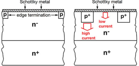
The use of pure Schottky junction diodes can achieve the lowest possible forward voltage, but problems may arise in high current situations, such as surge currents in some PFC applications. By embedding a P-doped region below the metal drift region of the Schottky structure, MPS diodes can improve surge current performance (Figure 1). In this way, a P-Ohmic contact is formed between the anode of the Schottky diode and the metal, and a P-N junction is formed with lightly doped SiC drift or epitaxial layers.
Structural comparison between SiC Schottky diode (left) and MPS diode (right)
Figure 1: The structural comparison between SiC Schottky diode (left) and MPS diode (right) is shown. (Image source: Vishay Semiconductor)
Under normal circumstances, the Schottky structure of MPS diodes conducts almost all of the current, and the characteristics of diodes are similar to Schottky diodes, with corresponding switching characteristics.
In the case of high transient surge current, the voltage across the MPS diode will rise and exceed the threshold voltage of the built-in P-N diode, thus starting to conduct and reducing local resistance. This will divert the current through the P-N junction region, thereby limiting power dissipation and reducing thermal stress on the MPS diode. Under high current conditions, the conductivity of the drift region increases, keeping the forward voltage at a lower value.
The surge current of SiC devices is due to their unipolar nature and relatively high drift layer resistance. The MPS structure can also improve this performance parameter, while the geometric position, size, and doping concentration of the doped P region will affect the final characteristics. Forward voltage drop is a compromise between leakage current and surge current rating.
Under reverse bias, doping the P region will force the entire maximum field strength region to move downwards, leaving the defective metal isolation layer and entering the almost defect free drift layer, thereby reducing the total leakage current. This enables MPS devices to operate at higher breakdown voltages under the same leakage current and drift layer thickness conditions.
Vishay's MPS structure adopts thin film technology, which reduces the thickness of the back of the diode structure through laser annealing. Compared with early solutions, it can reduce the forward voltage drop by 0.3 V. In addition, the forward voltage drop of the diode is almost independent of temperature (Figure 2).