
- 4E, No.3 Shenfeng Road, Liuyao Community, Henggang Street, Longgang District, Shenzhen,China
- cc.shen@xypltd.com
- Call: +86 15112667855
News
Improving the efficiency of high-performance switching converters using SiC power semiconductors
- 2026-09-28
Although silicon (Si) devices are relatively mature, silicon carbide (SiC) power devices are still expected to reduce product costs and improve efficiency. However, some designers may still consider SiC semiconductors to be quite expensive and difficult to control.
Taking Microchip Technology's SiC devices as an example, we will start with the basic advantages of SiC technology to dispel these concerns for you. Subsequently, we will explore SiC power semiconductors and showcase simulation tools, configurable digital gate drivers, and reference designs that help manage the development process.
Small size, light weight, high efficiency, and affordability
Many high-performance electrical applications in industrial plants, electric vehicles (EVs), or renewable energy must continuously improve energy conversion efficiency, save resources, and reduce costs. Compared with mature silicon insulated gate bipolar transistors (IGBTs), SiC MOSFETs have some outstanding advantages, with system voltages up to 2000 V and power levels exceeding 3 kW.
With the characteristics of steep switch edges and less overshoot, SiC semiconductor can achieve extremely low switching losses. At a switching frequency of 30 kHz, compared with IGBT, the switching losses can be reduced by up to 70% (Figure 1). This can improve system efficiency and reduce electromagnetic interference (EMI), thereby minimizing the need for power factor correction (PFC) and line filters.
Figure 1: Compared with IGBT (top), SiC MOSFET (bottom) can reduce switching losses by more than 70% at a switching frequency of 30 kHz. (Image source: Microchip Technology)
Working under high switching frequency, high voltage, and low current conditions requires the use of smaller inductive and capacitive components. This can reduce weight, decrease wire diameter, and lower BOM costs. Compared to silicon transistors, SiC semiconductors are more stable and have better heat dissipation performance under high temperature conditions, allowing for the use of smaller heat sinks to minimize volume as much as possible.
Due to the high avalanche energy, SiC MOSFETs exhibit very stable performance in non clamp inductive switching (UIS) applications. Overall, SiC MOSFETs are highly reliable, capable of achieving high power density and withstanding transient short circuits.
SiC Schottky barrier diode with fast speed and low loss
For designers who want to improve system efficiency, reduce external dimensions, and increase operating temperatures, Microchip Technology's SiC semiconductors provide an innovative choice suitable for applications such as photovoltaic inverters, battery charging, energy storage, motor drivers, uninterruptible power supplies (UPS), auxiliary power supplies, and switch mode power supplies (SMPS).
Microchip's SiC Schottky barrier diode (SBD) design features balanced surge current, forward voltage, thermal resistance, heat capacity, low reverse current, and low switching loss values.
SBD also offers discrete designs, such as the MSC050SDA070BCT dual SBD with a common cathode and TO-247-3 packaging structure, which can handle repeated reverse recovery voltage (VRRM) of 700 V and forward current (IF) of 88 A. The MSC50DC70HJ full bridge module uses threaded terminals and can handle 700 V voltage and 50 A current, while the MSCDC50X1201AG three-phase bridge module is designed specifically for through-hole welding applications.
Durable and sturdy high voltage, high current SiC MOSFET
The new SiC MOSFET has high UIS capability, approximately 10 to 25 J/cm2. A typical N-channel single transistor (such as MSC080SMA120B4) adopts the TO-247-4 packaging structure, which can switch 37 A current at a maximum voltage of 1200 V and has an independent Kelvin source connection, achieving interference free gate control.
SiC MOSFET power modules are highly suitable for switching converter applications in the two digit and three digit kilowatt range. For example, the MSCSM120AM02CT6LIAG half bridge module uses threaded terminals with extremely low leakage inductance. This device contains two N-channel MOSFETs that can safely switch load circuit voltages up to 1200 V and continuous currents up to 947 A.
The MSCSM120TAM31CT3AG three-phase half bridge module can handle drain to source voltage (VDSS) up to 1200 V, switch current (ID) up to 89 A, and maximum power dissipation (PD) of 395 W. The integrated SBD freewheeling diode has zero reverse recovery, zero forward recovery, and temperature independent switching characteristics.
Digital programmable gate driver
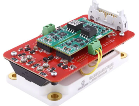
Microchip's Accelerated SiC Development Kit (ASDAK-MSCSM120AM02CT6LIAG-01) contains all the hardware and software components required to operate low inductance SiC modules. This kit provides a ready to use digital dual channel SiC gate driver plugin board, specifically designed for controlling 1200 V SiC modules. This gate driver can be programmed using Microchip's Intelligent Configuration Tool (ICT) and programming adapter to achieve optimal performance.
The driver board uses a suitable adapter card to directly insert into the SiC module, forming a compact half bridge unit that can achieve multi-level on/off operations (Figure 2). The gate driver supports advanced switch control, has powerful short-circuit protection function, and is fully configurable by software, including+/- Vgs gate voltage.