
- 4E, No.3 Shenfeng Road, Liuyao Community, Henggang Street, Longgang District, Shenzhen,China
- cc.shen@xypltd.com
- Call: +86 15112667855
News
How to use FPGA in resource constrained applications
- 2026-08-07
The demand for configurable logic in resource constrained embedded systems is increasing day by day. Applications such as edge AI, machine vision, and industrial automation require flexible application specific logic to meet constantly changing performance requirements while operating within strict power, size, and cost constraints. Modern field programmable gate arrays (FPGAs) can meet these competing requirements.
This article reviews the key design criteria to consider when selecting FPGA for resource constrained applications. Then, taking Altera's FPGA product portfolio optimized for power and cost as an example, explain how different product lines match specific application scenarios. Finally, the development kit and evaluation board that can be used for the development and validation of design concept prototypes were highlighted.
Precautions when choosing FPGA
Choosing FPGA for resource constrained systems requires considering multiple design requirements and matching the correct solution according to these requirements. There are several key FPGA features to consider:
Logic element (LE) capacity: As the basic component of FPGA, the number of logic elements determines how much customized logic can be implemented. The higher the quantity, the more complex the design becomes: a compromise is to increase power, cost, and packaging size.
I/O and Memory: FPGAs are typically used to connect different components in a system, so the number of I/O pins is an important consideration. In order to improve I/O performance, many FPGAs integrate reinforced fixed logic blocks for interfaces such as PCI Express (PCIe), high-speed storage, and gigabit transceivers.
In addition, some FPGAs also integrate components such as analog-to-digital converters (ADCs) and flash memory. These enhancement components can reduce the need for supporting chips, thereby saving circuit board space and improving energy efficiency.
Processor integration: It is possible to implement a "soft" microprocessor unit (MPU) within an FPGA instead of using an external processor. This method can reduce the size of the system, but it is most suitable for applications that do not require high workloads for MPU.
For applications that require MPU to have faster speed and higher efficiency, designers can consider using an FPGA with a hard core processor system (HPS) to implement the MPU as a fixed logic block in the FPGA.
Hardware Accelerator: FPGAs typically include dedicated digital signal processing (DSP) blocks that can effectively handle computationally intensive tasks such as motion control. High end devices may be equipped with metering blocks specifically designed for AI workloads. The functions of these accelerator blocks vary greatly among different FPGA series, which can greatly affect the overall performance of the system.
Packaging and power optimization: Some FPGAs are specifically designed to minimize physical and electrical footprint. For example, they can provide low-power sleep mode.
Tools: Creating custom logic is a daunting challenge, especially for novice designers. The emergence of tools such as Altera's Quartus Prime design software has simplified this process.
Quartus Prime provides a developer friendly experience, a wide range of pre built logic block directories, and the ability to automatically interconnect these logic blocks, making FPGA design easier to implement. This tool integrates commonly used AI and machine learning (ML) workflows, enabling developers to deploy popular operating systems (OS) such as Linux and Zephyr on FPGAs.
The above functions can greatly accelerate the design speed of FPGA, so tool functionality is also an important consideration when selecting devices.
High performance computing for advanced embedded workloads
To illustrate how design requirements affect FPGA selection, it may be helpful to start with high-end applications that require ultra-high computational density, bandwidth, and integration. Below, we will provide a detailed analysis using advanced edge AI applications and high-performance industrial gateways as examples.
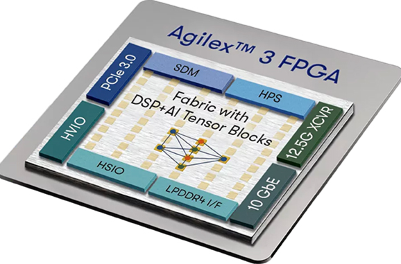
The Agilex 3 FPGA (Figure 1) is designed specifically to meet these application requirements and can provide up to 135K LE. These chips come in two types: pure FPGA and system on chip (SoC). SoC device integrates dual core 800 megahertz (MHz) Arm ® Cortex ®- A55, Enable FPGA to handle complex software stacks, such as human-machine interfaces (HMI) or network stacks.
This programmable structure features AI tensor blocks that can provide up to 2.8 trillion INT8 operations per second (TOPS). These tensor blocks support various computational formats, including FP16, FP19, FP32, and BFLOAT16, and have been optimized to achieve efficient execution of AI workloads. In addition, it also includes a variable precision DSP block that provides up to 180 Gigabyte Floating Point Operations per Second (GFLOPS) performance for general signal processing.