
- 4E, No.3 Shenfeng Road, Liuyao Community, Henggang Street, Longgang District, Shenzhen,China
- cc.shen@xypltd.com
- Call: +86 15112667855
News
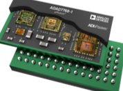
ADI's data acquisition solution shines in the field of advanced lithography chip manufacturing
- 2026-09-04
Driven by the expected increase in semiconductor chip sales from $600 billion in 2022 to $1 trillion in 2030, the semiconductor manufacturing equipment (SME) market is expected to achieve significant growth in the next five years. Sensors are the core of advanced lithography systems used in chip manufacturing.
When manufacturing complex, high-performance, and increasingly small semiconductor chips, it largely relies on high-precision and high-sensitivity photolithography processes, which help to print complex patterns on silicon wafers and other substrates used in chip manufacturing.
The advanced lithography system adopts extremely precise and sensitive technology, which not only increases process yield, but also minimizes waste and optimizes factory efficiency to the greatest extent possible. In order to achieve the necessary sub micron and nanometer level precision for large-scale production of integrated circuits (ICs), these systems rely on thousands of sensors to monitor and control position, temperature, energy, and movement.
The overall performance of the system depends on the precise and reproducible performance of each sensor. Advanced algorithms can interpret large amounts of sensor data and coordinate necessary adjustments in a very small but detailed way using thousands of actuators.
Analog Devices, Inc. (ADI) utilizes its signal chain micro module (µ Module) technology to provide a high-performance, miniaturized analog-to-digital data acquisition (DAQ) solution for monitoring photolithography semiconductor manufacturing subsystems, addressing the production challenges faced by wafer fabs and integrated device manufacturers.
Application Background
The continuous miniaturization of semiconductors has promoted the performance improvement from smart phones to supercomputers, as well as the processing requirements of generative artificial intelligence (GenAI), quantum computing, the Internet of Things and edge computing. To meet the requirement of continuously shrinking the size of semiconductors, advanced processes and innovative control systems must be adopted to reduce the width of circuits to one ten thousandth of a human hair.
Photolithography technology is a fundamental technique in semiconductor manufacturing, which can accurately draw feature patterns on silicon wafers and other substrate wafers to manufacture integrated circuits. It utilizes photomasks and powerful, extremely precise beams or radiation to transfer the details of chip design patterns onto wafers coated with photoresist material. The photoresist reacts with light and then processes the wafer with chemical agents to etch circuit paths on the wafer substrate. Multiple photomasks are used in the layering process.
Highly specialized and extremely complex photolithography semiconductor manufacturing systems can only be produced by a very small number of companies, who have the ability to address technological challenges and provide the expensive research and development investment needed for sustained innovation in this field.
ASML is an industry leader that dominates the advanced lithography technology market with its unique cutting-edge extreme ultraviolet (EUV) system, which is crucial for producing the most advanced chips. The company's most advanced system costs billions of dollars and is currently capable of producing chips with feature sizes less than 2 nanometers, providing more transistors for each chip and reducing the spacing between transistors. The company also offers a deep ultraviolet (DUV) system, which utilizes longer wavelengths and is suitable for the production of mid-range and traditional chips at nodes of 14 nanometers, 28 nanometers, and above, and is more cost-effective.
Other photolithography semiconductor manufacturing systems are produced by Canon and Nikon, focusing on DUV lithography and traditional techniques for manufacturing less advanced nodes used in microelectromechanical systems, power semiconductors, and industrial applications.
Achieve extremely high precision
The photolithography process requires extremely high precision to achieve sub micron level patterns. Sensors and actuators are crucial for maintaining accuracy and yield, driving continuous technological advancements and developing smaller, stronger, and more energy-efficient semiconductors.
Sensors play a crucial role in actuator control, providing real-time feedback, error correction, and environmental compensation
Position sensors measure the accurate positions of wafers, photomasks, and lenses
Vibration sensors detect and compensate for vibrations that may interfere with calibration
Environmental sensors monitor temperature, humidity, and air quality to minimize the impact of the environment on accuracy
Force sensors and strain sensors ensure that the actuator applies the correct force during calibration and positioning
Sensors provide important real-time data for closed-loop feedback to dynamically adjust actuators, ensuring alignment and pattern accuracy. They can detect deviations in real-time, prevent defects in the etched pattern of the wafer, and ensure complete alignment between the photomask and the wafer, which is crucial for multi-layer chip design. They are also crucial in minimizing delays caused by misalignment or rework.